
In the future, electronic components will permeate everything, creating a new and rapidly growing pollution problem. Therefore, future equipment needs to be environmentally friendly and have strong recycling options. The paradigm shift in semiconductor technology is predicted based on the application of more suitable materials that can meet these standards. Carbon based materials, especially diamond, are promising candidate materials.
In this review, the volume and surface characteristics of diamond are introduced in combination with its applications in power electronics, Quantum technology, bioelectrochemistry and MEMS. To enter the commercial market, a large number of diamond seeds and wafers will be required. Introduced their availability, quality and size, as well as the energy required for production. At present, the production energy consumption of CVD diamond is 100-250 times higher than that of silicon. This problem can be solved by using a new solid-state microwave source. The definition of ‘green diamond’ takes into account the requirements for energy and methane/hydrogen production. A brief discussion and comparison were made on the global diamond market and its potential compared to SiC and GaN.
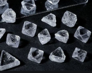
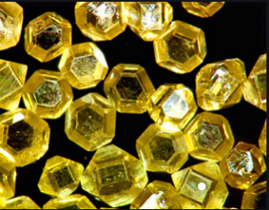
CVD diamond materials and gemstones are developing, and diamonds will become a global player. In 2021, the global synthetic diamond (HPHT and CVD) market size was around $14 billion, an increase of 8%. About 40% is attributed to high temperature and pressure, and 60% is attributed to CVD (polishing and roughness). This can be compared to the global diamond jewelry market of $65- $80 billion. By comparison, the global SiC market in 2021 was approximately $3 billion (compound annual growth rate of 11.7%), while the global GaN semiconductor device market in 2021 was $1.88 billion (compound annual growth rate of 24.4%). These numbers indicate the importance of diamond technology. Future research and development requires a roadmap to adjust the scientific and development progress of related equipment development. In order to produce diamond materials with wafer sizes (2-4 inches or larger), a new deposition system is required and will be used in conjunction with related etching, photolithography, stepping, and metallization technologies. Timely development requires intensive planning and communication.
CVD diamond technology is developing rapidly. The key and important step will be to produce diamond wafers with Electron mass. Here, the recent minimization of dislocation density has taken an important step, seemingly establishing control over defects and purity. Several companies are currently establishing large-scale diamond production based on embedded diamond or heteroepitaxial technology. Applications in MEMS or heat sinks do not have high requirements for defects. In the case of limited electronic and optical quality, they can become the “knockers” in wafer production. Over time, quality and wafer size improvements will be mandatory.
Prototypes of devices in Quantum technology, power electronics, electricity and bioelectrochemistry, MEMS and radiation detection have been realized. Most developments have reached the “prototype” level or TLR 4, which is the result of a lack of wafers. In order to establish a partnership with the company, the prototype equipment needs to demonstrate the potential for large-scale production. A demanding requirement is the availability of diamond wafers and the market. According to literature, market expectations can be summarized as follows:
(1) In 2023, the global diamond NV center magnetometer market will approach $160 million (with a compound annual growth rate of 7.9%).
(2) The market size of artificial diamond nanoparticles will reach 140 million US dollars in 2025 (with a compound annual growth rate of 12.4%).
(3) In 2023, the power electronics market size for 3kV diodes was $35 million.
If diamond wafers are available in a timely manner, these markets can be addressed through diamond devices.
The new applications with large markets are heat sinks ($32 million in 2020) and MEMS ($1.15 billion in 2019), both of which have high requirements. There is a huge mismatch in thermal expansion coefficient between AlScN/diamond based MEMS and GaN/diamond based 5G amplification station heat sink, making it difficult to combine. New technologies such as wafer bonding can solve this problem. In addition, certain applications require commercialization of 8-inch or larger wafers and integration with other materials such as AlScN. In addition, filters in these devices, especially 5G communication devices such as mobile phones, need to be cheap. Finally, the quantum applications of diamond are very attractive, demonstrating the largest global market. Diamond is unique in this field, but it requires large-scale production to enter and penetrate these markets.
In summary, CVD diamond technology has made good progress in diamond quality, doping, 3D forming, wafer production and optimization, and device prototype design. The market for diamond applications is clear and promising. The key improvements needed are: reducing the cost of diamond deposition technology, and establishing diamond wafers for large-scale production. These two themes will be bottlenecks for future success.


Here is your enquiry list